Hot Keywords:


Laminate:EMC, ITEQ, SYL, Isola, Rogers, Arlon,Nelco, Taconic, Hitachi, etc.
Chemical Solvent : Rohm&Haas (US) Atotech (Germany) Umicore (Germany)
Solder Mask:Taiyo (Japan) Dry Film : Asahi (Japan), Dupont (US)
lines matching up withdifferent industries.
S&L is one of the fewer PCB manufacturers that has full range of in
house surface treatment lines for ENIG,immersion,
silver,immersion tin,OSP,HASL, electrical gold plating,
electrical hard gold plating, electrical tin plating, electrical silver plating.


Maximum Layer Count: 40L Maximum Board Thickness: 7.0mm
Maximum Aspect Ratio: 12:1 Maximum Copper Thickness: 6OZ
Maximum Working-Panel Size: 2000x610mm Min. 4L Board Thickness: 0.38mm
Mechanical Hole / Land: 0.20/0.40mm Hole to Copper Registration Accuracy: +/-0.05mm
Hole Size Tolerance of PTH: +/-0.05mm Minimum Line Width/Space: 0.075/0.075mm
stabilize high quality performance
IPC standard implemented to ensure 100% FQC pass rate
PDCA cycle methodology in place for continuous improvement
Advanced Ion Chromatograph System (DIONEXICS-900)and
temperature cycle tester
guarantee outstanding reliability and stability.
Engaging in PCB R&D and manufacturing for 12 years, helping customer to optimize PCB design
We have 400 engineers who are experienced in PCB industry
over 9 years and familiar with industry standards.
We are awarded as national hi-tech enterprise, holding 7 ISO certificates and 71 IP patents.
Clean Production Enterprise in Canton. Leading Enterprise of Waste Reduction in Shenzhen City,Green PCB Factory.


Advanced automatic process lines: Universal VCP, Burkle lamination machine(Germany), Mitsubishi Laser Drilling machine, Hitachi Mechanical drilling machine, Screen automatic exposure machine (Japan),Screen LDI and AOI (Japan)


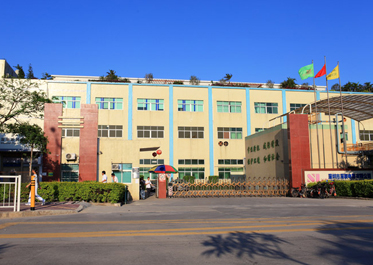
S&L Circuits was founded in 2002 and operates 2 factories in Shenzhen and Ganzhou respectively, 2600 employees in total. The factory floor area is 60,000M2 and total investment is $170million. S&L Shenzhen focus on rigid PCB and provide fast lead time for volume order. Lead time for double layer PCB requires 6-7 days and 9-12 days for 4 to 8 layers.Application distribution covers Telecom, Power supply, Security surveillance, Photoelectric module, Industry control, Medical and health care, Autom...

 Company:
*
 Phone:
*
  Email :
*
 Sun & Lynn circuit focus PCB R & D and manufacturing for 12 years
MoreInfo >>Hello! Sun & Lynn circuit is a professional engaged in high-end printed...
MoreInfo >>What do you Sun & Lynn circuit with well-known enterprise cooperation?
MoreInfo >>Since the plant S&L through a series of certification
MoreInfo >> Events in S&L
German customer RRC visited S&L on Aug.13, 2014 for on-site audit. RRC is specialized in power supply and rechargeable batteries that widely used in medical, military and consumable products.
 Industry Briefing